In the evolving landscape of quantum computing, the crucial yet often overlooked metric of device yield is coming to the fore, especially as the industry gears towards making quantum processors more accessible and financially viable. A seminal example of this shift in focus is Intel Corporation’s strategic advances in quantum research and development, leveraging its semiconductor expertise to address the yield challenges inherent in quantum computing manufacture.
Intel’s selection of spin qubits over alternative technologies such as superconducting qubits is a calculated move. This choice is primarily due to the significant reduction in die area per qubit, a parameter analogous to the cost-determining factors in traditional semiconductor chip production. However, the advantages in die area necessitate that the quantum bits maintain both high coherence times and gate fidelities to be feasible for quantum computing.
To expedite the process development towards achieving these high standards, Intel has embarked on a collaboration with BlueFors and Afore to create a custom cryogenic wafer prober. This innovative prober can cool test wafers to a brisk 1.6 K in about two hours, facilitating the rapid testing of thousands of spin qubits on a single 300 mm wafer.
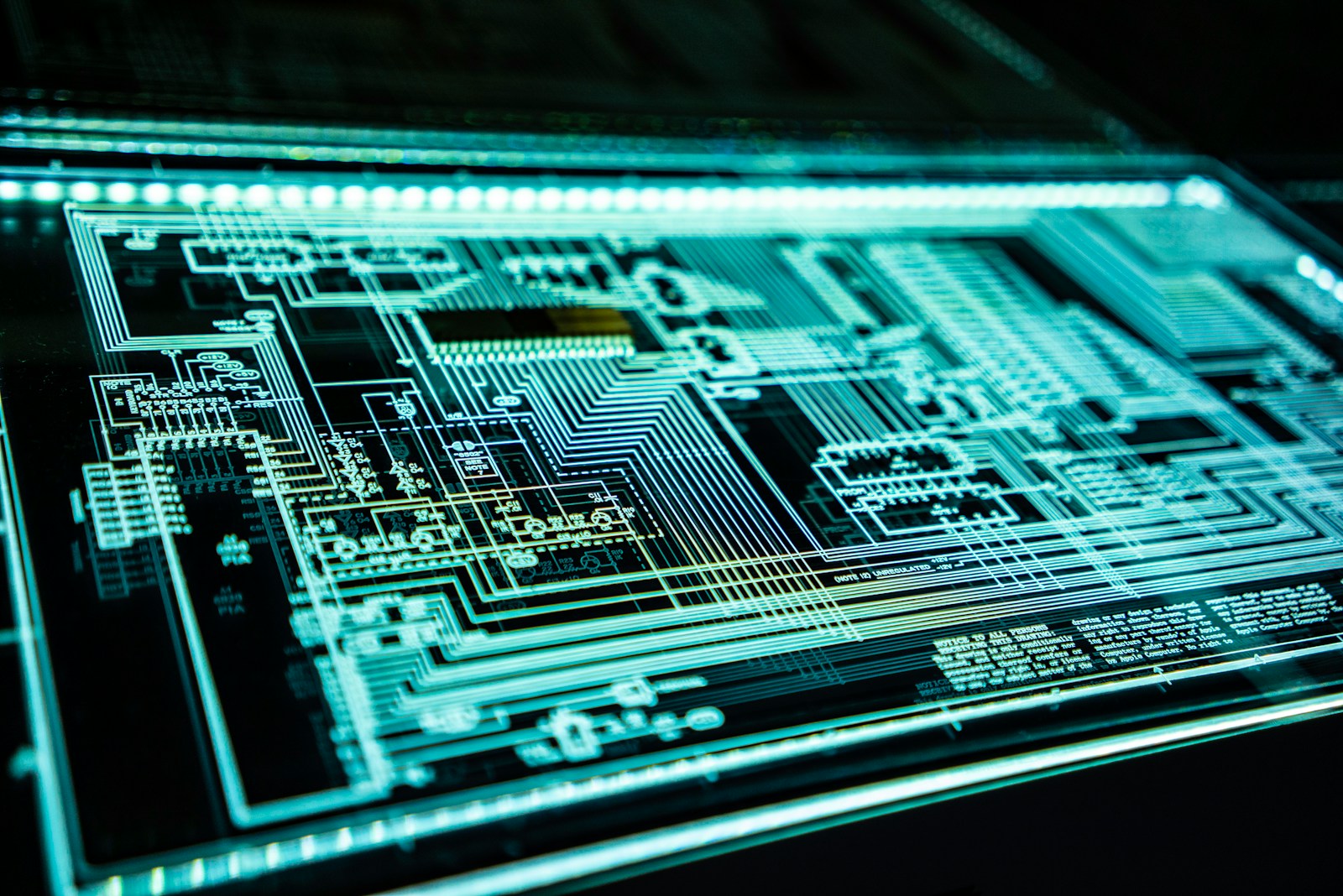
Intel’s endeavors with the Tunnel Falls chip, which contains 12 quantum dot sites arranged linearly, exemplify their progress in the field. Recent publications by the company showcase a promising 96% yield rate on wafers filled with multiple chips housing their quantum dot array. This yield is pivotal, as the next steps involve transitioning from a linear qubit arrangement to a more complex 2D structure, necessary for scaling up qubit numbers and enhancing connectivity.
At the heart of Intel’s quantum thrives the integration of Si/Ge epitaxial layers in their base wafers, diverging from the conventional Si-Mos layers used in standard semiconductors. This modification is intended to diminish the disorder within the qubits, optimizing their performance.
The accomplishments of Intel in this domain are not just a testament to their innovative prowess but also serve as a beacon for the quantum computing industry at large. As depicted in the chart demonstrating a high yield rate of spin qubit wafers, Intel’s approach underscores the imperative transition from merely achieving operational quantum processors to rendering them economically feasible on a larger scale.
Detailed technical insights into Intel’s quantum computing advancements have been documented in Nature, alongside a comprehensive blog article on Intel’s official website. These publications not only highlight the technical strides made but also Intel’s commitment to contributing to the broader quantum computing ecosystem.
As the quantum computing industry continues its march towards mainstream applicability, the focus on yield and cost-effectiveness championed by Intel may well pave the way for the next era of quantum technology development. With initiatives aimed at increasing the connectivity and number of qubits, alongside optimizing manufacturing processes, the future of quantum computing looks both promising and pragmatically attainable.
Source