Insider Temporary
- South Korean researchers have efficiently developed know-how to mass-produce quantum dot lasers.
- Electronics and Telecommunications Analysis Institute (ETRI) introduced that they’ve developed the know-how utilizing Metallic-Natural Chemical Vapor Deposition (MOCVD) programs.
- Quantum dot laser diodes had been historically produced utilizing Molecular Beam Epitaxy (MBE), however this methodology was inefficient.
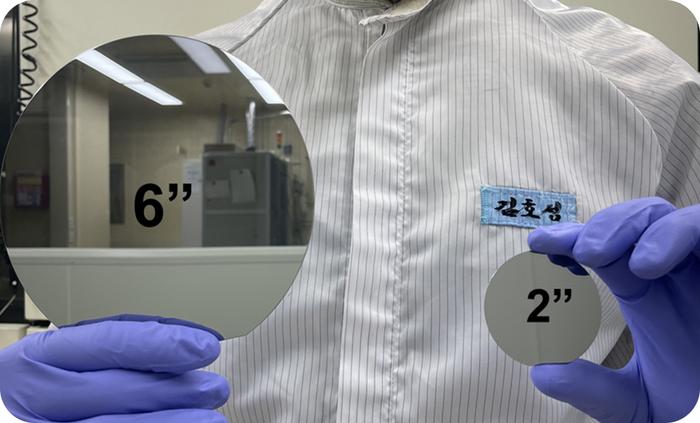
- Picture: Comparability of 2-inch and 6-inch compound semiconductor substrates. (ETRI)
PRESS RELEASE — South Korean researchers have efficiently developed know-how to mass-produce quantum dot lasers, broadly utilized in information facilities and quantum communications. This breakthrough paves the way in which for decreasing the manufacturing value of semiconductor lasers to one-sixth of the present value.
Electronics and Telecommunications Analysis Institute (ETRI) introduced that they’ve developed, for the primary time in Korea, know-how to mass-produce quantum dot lasers, beforehand solely used for analysis, utilizing Metallic-Natural Chemical Vapor Deposition (MOCVD) programs.
The ETRI Optical Communication Elements Analysis Part has efficiently developed indium arsenide/gallium arsenide (InAs/GaAs) quantum dot laser diodes on gallium-arsenic (GaAs) substrates, that are appropriate for the 1.3 µm wavelength band — theOptical Communication Wavelength Band is 1260~1360nm — utilized in optical communications.
Historically, quantum dot laser diodes had been produced utilizing Molecular Beam Epitaxy (MBE), however this methodology was inefficient attributable to its gradual progress velocity, making mass manufacturing difficult. By using MOCVD, which has greater manufacturing effectivity, the analysis staff has considerably enhanced the productiveness of quantum dot laser manufacturing. Quantum dot lasers are identified for his or her glorious temperature traits and robust tolerance to substrate defects, permitting for bigger substrate areas and consequently decrease energy consumption and manufacturing prices.

The newly developed quantum dot manufacturing know-how boasts excessive density and good uniformity. The produced quantum dot semiconductor lasers demonstrated steady operation at temperatures as much as 75 levels Celsius, exhibiting a world-leading achievement within the outcomes obtained through MOCVD.
Beforehand, optical telecommunication units used costly 2-inch indium phosphide (InP) substrates, leading to excessive manufacturing prices. The brand new know-how, utilizing GaAs substrates, that are lower than one-third the price of InP substrates, is projected to scale back the manufacturing value of communication semiconductor lasers to lower than one-sixth.
This know-how’s capability to make use of large-area substrates allows important reductions in course of time and materials prices.
The analysis staff plans to additional optimize and confirm this know-how to boost its reliability and switch it to home optical communication corporations. These corporations will obtain key know-how and infrastructure assist via ETRI’s semiconductor foundry, accelerating the commercialization timeline.
The anticipated discount in growth time and manufacturing prices will improve product worth competitiveness, probably growing market share internationally. This development is predicted to spice up the home optical communication element business.
In fashionable society, optical communication serves because the spine of our business. The analysis staff’s achievement is about to revolutionize the event of optical sources, connecting condominium complexes to giant cities and undersea optical cables.
Professor Dae Myung Geum from Chungbuk Nationwide College, a participant on this analysis, remarked, “The mass manufacturing know-how for quantum dots can considerably decrease the manufacturing prices of high-priced optical communication units, enhancing the competitiveness of the nationwide optical communication element business and contributing considerably to fundamental science analysis.”
Dr. Ho Sung Kim from ETRI’s Optical Communication Elements Analysis Part acknowledged, “This analysis consequence is a chief instance of securing each industrial viability and elementary innovation, probably altering the paradigm of the semiconductor laser business for optical communications.”


